.png?h=1080&iar=0&w=1920&hash=7DE0C34D177EB3E1035552C484579EBB)
PCB Layout Software from Xpedition eliminates data loss when jumping between tools to complete work
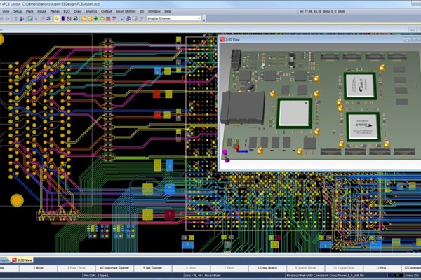
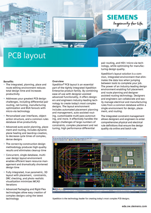
Xpedition PCB Layout Design Software combines ease of use with highly automated features to provide layout PCB designers with industry-leading advanced technologies to create the most complex designs.
Designers and engineers can easily collaborate and manage electrical and production rules from a common database in a single environment for design, placement, and routing.
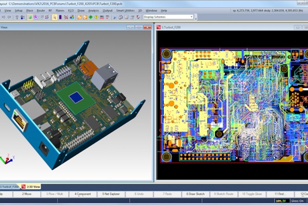
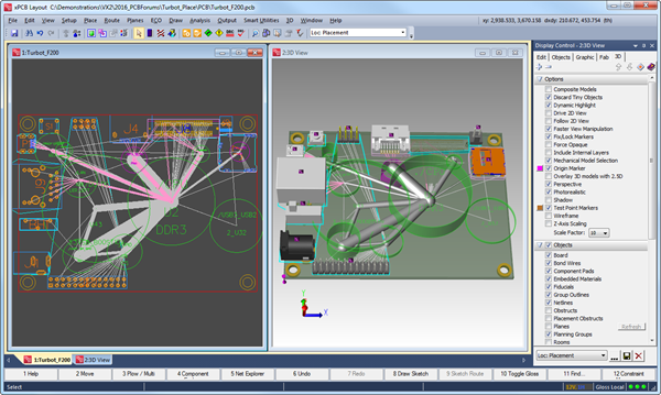
Xpedition Pcb Layout Software: a single, integrated editing environment
Xpedition PCB Layout Design Software is a key part of the Siemens ecosystem of electronics solutions. Reduces total design time and increases productivity with a single environment that can be customized to suit the way you design.
Design Reuse
Design reuse in Xpedition PCB Layout Design Software automates the process of copying circuits to reduce the overall time of the PCB design cycle while improving quality by using known IPs.
The built-in copy-circuit functionality allows circuits to be copied and pasted within and between projects with advanced equivalence algorithms to automatically map schematic logic to the circuit during the copy process. In addition, the use of group planning and placement makes project reuse even more powerful.
A formal design reuse module creates and stores reusable blocks of circuits-including schematic and PCB placement and routing data-in a central library. This IP can be shared across the enterprise and can be placed and modified within the same project and in multiple projects.
Design Collaboration
Engineering design changes can cause delays and introduce errors. Design collaboration in the layout PCB software Xpedition eliminates barriers that limit changes within a schematic flow/layout.
Whether it is a single schema designer or multiple schema designers collaborating, Xpedition supports concurrent changes in constraints and logic while the layout is in progress, synchronizing schema and layout with powerful integration functions.
Modifications made to the schema and/or layout are easily updated in a common database without interrupting the design cycle. PCB designers also have access to a schematic view embedded within the layout tool
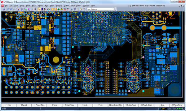
Simultaneous group design
The Xpedition team's award-winning layout, based on Xtreme technology, allows multiple designers to work simultaneously within a single layout PCB design database.
For PCB designs that have aggressive schedules, simultaneous layout enables collaboration among geographically dispersed or functionally organized PCB design teams to maximize productivity and dramatically reduce project time to market.
It is designed for immediate deployment and is fully functional like its single-user counterpart. There is no time-consuming training required, no changes to a company's infrastructure or library to implement. Refer to the Xpedition xPCB Team Layout data sheet for complete details.
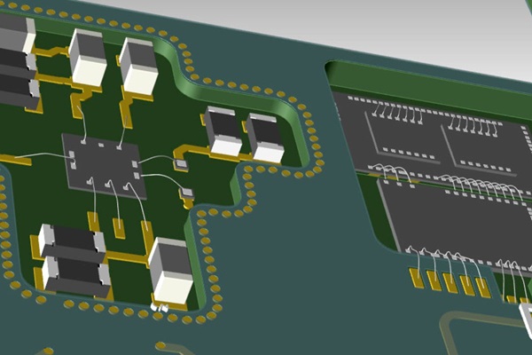
Advanced Packaging
Usually, die-level packaging design is done in a separate tool, but with Xpedition, incorporating die-level packaging into your layout using wire bonding technology is available in the same integrated database.
Advanced constraint definitions for cavity, chip-on-board, and multi and stacked-dies design are maintained in the built-in constraint manager. Easy-to-use wizards are provided to create advanced die bond models, and wire bonds can be validated for DRC errors using 3D visualization.
Advanced constraint definitions for cavity, chip-on-board, and multi and stacked-dies design are maintained in the built-in constraint manager. Easy-to-use wizards are provided to create advanced die bond models, and wire bonds can be validated for DRC errors using 3D visualization.
Embedded passive/Active design
PCB Xpedition layout software automates the creation of layouts with embedded passive/active components that previously required weeks of manual effort. As ICs and FPGAs increase in speed and density, they require more passive components (resistors and capacitors)-some may need several hundred.
Implementing these as embedded components over discrete SMDs can significantly reduce board size and improve performance. A complete embedded solution is provided: trade-off tools decide which components can be implemented as embedded based on board size and cost, passive material choices, automatic synthesis guided by material supplier libraries, and complete manufacturing data generation.
Built-in active components can also be used in your more advanced designs.
Siemens SW Xpedition PCB layout
Download the data sheet of Xpedition PCB Layout to learn more about its full capabilities.
Learn about all the features of Xpedition Enterprise for PCB Design, Simulation, and DFM